Toward Isotropic Metamaterials [Feb 15, 2009]
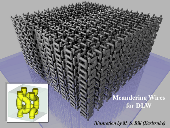
Illustration of our blueprint design for DLW and CVD.
We published in Optics Letters the first truly bulk one- and two-dimensionally isotropic photonic negative index metamaterials (NIMs), which can potentially be fabricated with direct laser writing (DLW) processes around telecom wavelengths with about 20THz bandwidth [1]. Direct laser writing is considered as the most viable technique for the fabrication of truly 3D large-scale photonic metamaterials [2].
All photonic metamaterials at terahertz frequencies have been fabricated by well-established two-dimensional fabrication technologies, such as electron-beam lithography and evaporation of metal films, but they are one-dimensional designs with only few functional layers [3,4]. However, full isotropy is essential for the realization of Pendry's perfect lens [5]. Designs of 3D isotropic NIMs exist, but fabricating them has remained a challenging task.
DLW processes enable computer-controlled formation of arbitrary three-dimensional patterns, which are not possible to fabricate with traditional photolithographic processes [6,7]. Patterns are usually obtained by either rastering the beam above a fixed surface or by moving the substrate. Length scales of generated individual 3D volumes of materials span six orders of magnitude, from nanometers to millimeters. In contrast to lithography, directed self-assembly or other patterning approaches, DLW does not require masks or pre-existing patterns. Therefore, it can be also considered as a 'rapid prototyping' tool. Laser sources for DLW ranges from ultrafast femtosecond-pulsed lasers to continuous wave lasers such as solid-state, gas, fiber, or semiconductor lasers. For example, a diode laser, which induces a phase transition between crystalline and amorphous material (i.e., DLW modification), is used to rewrite a compact disc. [6]
In the manufacturing of electronic and optoelectronic devices such as cell phones, digital cameras, and laptop computers, DLW is an established technology, especially for laser drilling of via holes for stacked or built-up printed circuit boards. DLW can also be used to trim or pattern thin metal films on the microelectromechanical structures, which is otherwise difficult to process by conventional techniques due to extreme topography and/or fragility. DLW with multibeam parallel processing can be employed to achieve high throughput in mass production. [7]
Our collaborators in Prof. Martin Wegener's group in Karlsruhe, Germany [2] have recently demonstrated the feasibility of this technique at near-IR frequencies assisted with silver chemical vapor deposition. However, there has been a clear need to come up with a better design that is suitable for DLW. [8] Currently we continue to work with Prof. Wegener's group toward the fabrication of our blueprint designs.
References
[1] D. O. Guney, Th. Koschny, M. Kafesaki, and C. M. Soukoulis, Connected bulk negative index photonic metamaterials, Opt. Lett. 34, 506 (2009).
[2] M. S. Rill, C. Plet, M. Thiel, I. Staude, G. von Freymann, S. Linden, and M. Wegener, Photonic metamaterials by direct laser writing and silver chemical vapour deposition, Nature Mater. 7, 543 (2008).
[3] G. Dolling, M. Wegener, and S. Linden, Realization of a three-functional-layer negative-index photonic metamaterial, Opt. Lett. 32, 551 (2007).
[4] N. Liu, H. Guo, L. Fu, S. Kaiser, H. Schweizer, and H. Giessen, Three-dimensional photonic metamaterials at optical frequencies, Nature Mater. 7, 31 (2008).
[5] J. B. Pendry, Negative refraction makes a perfect lens, Phys. Rev. Lett. 85, 3966 (2000).
[6] C. B. Arnold and A. Pique, Laser direct-write processing, MRS Bulletin 32, 9 (2007).
[7] K. Sugioka, B. Gu, and A. Holmes, The state of the art and future prospects for laser direct-write for industrial and commercial applications, MRS Bulletin 32, 47 (2007).
[8] E. Ozbay, The magical world of photonic metamaterials, Optics Photonics News 19, 22 (2008).