Thermal Imaging
Abstract: In this project we develop high resolution thermal imaging systems. As a part of our work we have designed a two-dimensional (2D) photonic band gap (PBG) structure for the temperature mapping of ultra-small structures, such as microelectromechanical systems (MEMS). The operational principle of the device is based on guiding and selecting the specifically tuned wavelengths through the corresponding cavities. We have shown that having processed the intensities, obtained from each cavity, in accordance with the blackbody radiation characteristics and the transmission properties of the structure, the temperature reading of the target in concern can be obtained. Despite many studies concerning guided modes in 2D PBG materials, few such sensor applications are proposed.
Keywords: Thermal Imaging, Photonic Crystals
Collaborators: Naci Inci (Bosphorus University)
Surface temperature measurements have many applications in the physical and environmental sciences. Temperature sensors that depend on the attainment of thermal equilibrium with a surface via conductive or convective heat transfer are problematic and hard to implement in miniature systems, because they require intimate contact with the surface, which is destructive and affects the local surface energy balance and thus the temperature. Furthermore, such sensors are themselves affected by radiant energy exchange that can cause their temperature to differ from the surrounding surface [1].
Fortunately, the capabilities of non-contact/non-destructive IR thermometry that we study in this project offers an alternative approach, even when compared to the conventional IR thermometry, for the temperature mapping of delicate and miniature components such as MEMS, where the control and reliability is quite important.
In the last century, the control over electrical properties of materials led to transistor revolution in electronics. Now, in this century, photonic crystals inspired great interest to control the flow of light. Photonic band gap (PBG) materials seem to be more promising as a base medium both for future laser based photonic integrated circuits and more advanced quantum network technology [2-3].
The capabilities of perfect periodic arrangements of dielectric materials (i.e., photonic crystals) to control the propagation of electromagnetic waves have been well studied since the primary predictions of Yablonovitch and John [4-10]. In analogous to crystalline solids with a periodic potential for electronic wavefunctions, photonic dispersions are strongly perturbed by the spatial periodicity of dielectric function in the photonic lattice. The strongest effect is experienced at the high symmetry points of the photonic Brillouin zone where energy gaps with no propagating states exist. The size of these gaps depends on the refractive index contrast, the filling fractions of the dielectric media and some other parameters of the lattice [11].
A line-defect can be introduced into the PBG material by adding, removing or distorting material in the crystal. These defects break the above symmetry and may give rise to the otherwise not allowed defect states within the PBG region of the photonic crystal. It is well known that introducing defects in electronic bandgap materials allow the electronic wavefunctions to have an energy in the electronic bandgap. Thus, the electronic wavefunction is localized around the impurity. Similarly, introducing defects in PBG materials, one can localize and control the properties of wavefunctions, thus making these materials ever more useful. Defect states appear as spikes in the PBG region transmission response [4,12]. One can also use point defects in photonic crystals to trap light [2,13]. Therefore, the electromagnetic wave with a frequency in the gap can be guided along the line defect from one location to another without appreciable losses [2,14] and the thermal imaging application in this project is mostly based on this peculiar property of photonic crystal (or PBG) waveguides.
In contrast to the conventional waveguides, the mechanism of confinement within the PBG waveguide is not due to the total internal reflection, but could be explained by an optical quantum well which does not allow the modes within the surrounding region of the waveguide. This is the reason why light becomes confined to the modes within the PBG [15].
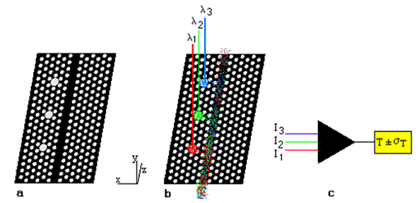
As a part of our thermal imaging project we considered a 2D PBG slab which consists of triangular array of air holes etched into the substrate with one straight waveguide and isolated point defects, shown in Fig. 1a. Because it is lossless through the spectral region chosen, optical properties of GaAs are used in the Finite-Difference-Time-Domain (FDTD) simulations.
The transduction mechanism, as shown in fig. 1b, of the PBG device is based on guiding and filtering out of specifically tuned three optical wavelengths transmitted through the waveguide. After the optical intensities of chosen wavelengths were scaled in accordance with the blackbody radiation characteristics, the surface temperature reading of the target can be obtained. In our analysis, we demonstrated that the transmission response of the considered structure allows such scaling.
Figure 1 The photonic cystal structure and its transduction mechanism (a) 2D triangular lattice of air holes etched into GaAs with one line-shaped defect and three isolated point defects. Lattice constant, a, is 0.382-nm and radius to lattice constant ratio, r/a, is 0.3. (b) Guiding and filtering out of the certain wavelengths from the corresponding specifically tuned isolated point defects. (c) Scaling of optical intensities corresponding to the chosen wavelengths in accordance with the blackbody radiation characteristics.
Many studies have been carried out concerning guided modes in the 2D PBG materials [5,6,11,14,16,17]. However, very few studies can be found in the literature concerning such sensor applications. In this project we collaborate with Bosporus University, Turkey.
References
[1] J. M. Baker, J. M. Noman, A. Kano, A new approach to infrared thermometry, Agricultural and Forest Meteorology 108, 281-292 (2001).
[2] J. D. Joannopoulos, R. D. Meade, J. N. Winn, Photonic Crystals: Molding the Flow of Light, Princeton University Press (1995).
[3] O. Painter, R. K. Lee, A. Scherer, A. Yariv, J. D. O'Brein, P. D. Dapkus, I. Kim, Two-Dimensional Photonic Band-Gap Defect Mode Laser, Science 284, 1819 (1999).
[4] A. L. Reynolds, H. Chong, I. G. Thayne, P. J. I. de Maagt, J. M. Arnold, Transmission response for in-plane and out of plane propagation for a 2D photonic crystal with a planar cavity, Synthetic Metals 116, 433-437 (2001).
[5] M. Loncar, T. Doll, J. Vuckovic, A. Scherer, Design and fabrication of silicon photonic crystal o optical waveguides, Journal of Lightwave Technology 18, 1402-1411 (2000).
[6] S. G. Johnson, S. Fan, P. R. Villeneuve, J. D. Joannopoulos, Guided modes in photonic crystal slabs, Physical Review B 60, 5751-5758 (1999).
[7] E. Yablonovitch, Physical Review Letters 58, 2059 (1987).
[8] S. John, Physical Review Letters 63, 1950 (1989).
[9] S. Kim, V. Gopalan, Strain-tunable photonic band gap crystals, Applied Physics Letters 78, 3015-3017 (2001).
[10] C. Liguda, G. Botger, A. Kuligk, R. Blum, M. Eich, H. Roth, J. Kunert, W. Morgenroth, H. Elsner, H. G. Meyer, Polymer photonic crystal slab waveguides, Applied Physics Letters 78, 2434-2436 (2001).
[11] I. S. Culshaw, V. N. Astratov, R. M. Stevenson, D. M. Whittaker, M. S. Skolnick, T. F. Krauss, R. M. De La Rue, Determination of the band structure of photonic crystal waveguides, Physica E 7, 650-655 (2000).
[12] T. Sondergaard, A. Bjarklev, J. Arentoft, M. Kristensen, J. Erland, J. Broeng, S. E. Barkou Libori, Designing finite-height photonic crystal waveguides: confinement of light and dispersion relations, Optics Communications 194, 341-351 (2001).
[13] S. Noda, A. Chutinan, M. Imada, Trapping and emission of photons by a single defect in a photonic bandgap structure, Nature 407, 608-610 (2000).
[14] M. Qiu, S. He, Guided modes in a two-dimensional metallic photonic crystal waveguide, Physics Letters A 266, 425-429 (2000).
[15] M. D. B. Charlton, M. E. Zoorob, G. J. Parker, M. C. Netti, J.J. Baumberg, S. J. Cox, H. Kemhadjian, Experimental investigation of photonic crystal waveguide devices and line-defect waveguide bends, Materials Science and Engineering B 74, 17-24 (2000).
[16] C. J. M. Smith, R. M. De La Rue, H. Benisty, U. Oesterle, T. F. Krauss, D. Labilloy, C. Weisbuch, R. Houdré, In-plane microcavity resonators with two-dimensional photonic bandgap mirrors, IEE Proc.-Optoelectron. 145, 373-378 (1998).
[17] K. M. Ho, C. T. Chan, C. M. Soukoulis, Existence of Photonic Gap in Periodic Dielectric Structures, Physical Review Letters 65, 3152-3155 (1990).