Losses in Metamaterials
Abstract: In this project we explore the physical mechanisms of losses in metamaterials, develop new circumventing strategies and turn them into manufacturable designs. We study all frequency regions ranging from GHz to THz and visible. Reducing the losses, especially, in optical frequencies is critical to many exotic applications expected from metamaterials technology, such as ultra-high resolution imaging and electromagnetic invisibility cloaks.
Keywords: Metamaterials
Collaborators: Costas Soukoulis (Ames Laboratory), Thomas Koschny (Ames Laboratory), Philip Evans (Oak Ridge National Laboratory), Sahin Kaya Ozdemir (Washington University, St. Louis), and Lan Yang (Washington University, St. Louis)
Support: NSF, ONR (current); DOE, USAFOSR, DARPA, ONR, FET, ORAU, ORNL (past)
In this project we explore the physical mechanisms for losses in metamaterials, develop new circumventing strategies and turn them into manufacturable designs. We study all the frequency regions ranging from GHz to THz and visible. Reducing the losses, especially, in optical frequencies is critical for many fascinating applications.
Plasmon Injection Scheme
Metamaterials have led to previously unthought of applications such as a flat lens [1], perfect lens [2], hyperlens [3–5], ultimate illusion optics [6–8], perfect absorber [9,10], optical analog simulators [11,12], metaspacers [13], and many others. Despite tremendous progress in theory and experimental realizations, the major current challenges seem to further delay the metamaterial era to come. For instance, achieving full isotropy, feasible fabrication methods, broad bandwidth, and compensation of dissipative losses especially at optical frequencies are among the challenges yet to be solved [14,15]. Perhaps the most critical of all is how to avoid optical losses—especially in large-volume structures. The performance of devices utilizing metamaterials dramatically degrades at optical frequencies due to significant Ohmic losses arising from the metallic constituents. The strategies proposed to mitigate the losses include passive reduction and active compensation schemes. Avoiding sharp edges [16], reducing skin depths [16–18], and classical analog of electromagnetically induced transparency are proposed as passive loss minimization techniques [19,20]. Constitutive materials such as dielectrics [21], nitrides [22], oxides [23], graphene [24], and superconductors [24–30] have also been explored for possible alternatives to lossy conductors. However, so far none of these materials has been shown to outperform the performance of high-conductivity metals at room temperature [31,32]. Active compensation of losses using a gain medium has emerged as the most promising strategy to avoid the deleterious impacts of losses on metamaterial devices. Optically pumped semiconductor quantum dots and quantum wells incorporated in planar metamaterials have been experimentally shown to compensate the losses to some extent [33–38]. A remarkable improvement in the figure of merit (FOM) of a negative refractive index of a fishnet metamaterial operating in the visible range has been recorded using dye molecules embedded in epoxy resin and pumped by picosecond pulses [35,37]. Although important progress has been made in theory [14,15,34,35,38–40] and experiments [14,15,33,36,37,41–43], there still exist concerns about the viability of active compensation of loss by gain medium for practically large-volume metamaterials [14]. First, it was shown that causality and the stability of the system make the loss compensation difficult without compromising interesting properties of the metamaterials [14,44,45]. Second, the requirement for optical or electrical pumping makes the metamaterials complex and dependent on available pump sources or gain materials at particular wavelengths. Third, high maintenance and the short chemical life of the dye molecules make the durable metamaterials unfeasible [35,37].
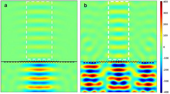
As part of this project, we explore a novel optical amplification technique to compensate and control losses in metamaterials [46]. Our amplification scheme is ideally suited for compensating losses in metamaterials operating in the visible spectrum and is fundamentally different from major amplification schemes based on stimulated optical emission, Raman scattering, and optical parametric amplification, or recently proposed surface plasmon polariton (SPP) amplification for plasmonic integrated circuits [43]. It does not require gain medium, interaction with phonons, or any nonlinear medium, and it operates at room temperature. Our technique relies on the constructive interference of externally injected SPPs within the metamaterial to coherently amplify the domestic SPPs of the metamaterial. The amplified SPPs are then coupled into the free space via an appropriately designed grating network at the output port of the metamaterial (see Fig. 1). We have shown that this proposed scheme, referred to as the plasmon injection (PI or Π) scheme, provides diverging FOM, hence, loss-free optical metamaterials without using an optical gain providing medium.
Figure 1 Compensation of losses and amplification in the negative index metamaterial. Wave propagation through finite period negative index metamaterial at with a refractive index of −1 (i.e., at 562THz) (a) without auxiliary sources (i.e., no loss compensation) and (b) with auxiliary sources (i.e., loss compensation). The surface plot shows magnetic field distribution. The boxed region indicates the transmitted output of the negative index metamaterial.
Acknowledgment
In the past, our project in part was supported at Ames Laboratory by the Department of Energy (DOE) (Basic Energy Sciences). It was also partially supported by the United States Air Force Office of Scientific Research (USAFOSR), by Defense Advanced Research Agency (DARPA), Office of Naval Research (ONR), and European Community Future and Emerging Technologies (FET) project Photonic Metamaterials (PHOME). Additionally, the project was supported by ORAU Powe Award and through user-access-grant for CNMS facilities at Oak Ridge National Laboratory (ORNL). Currently, the project continues under NSF Grant ECCS-1202443 and ONR grant (award N00014-15-1-2684). Our collaborators include Lan Yang and Sahin Kaya Ozdemir at Washington University, St. Louis, Philip G. Evans at ORNL, Costas Soukoulis and Thomas Koschny at Ames Laboratory.
References
[1] V. G. Veselago, Sov. Phys. Usp. 10, 509 (1968).
[2] J. B. Pendry, Phys. Rev. Lett. 85, 3966 (2000).
[3] Z. Liu, H. Lee, Y. Xiong, C. Sun, and X. Zhang, Science 315, 1686 (2007).
[4] X. Zhang and Z. Liu, Nat. Mater. 7, 435 (2008).
[5] R. Junsuk, Z. Ye, Y. Xiong, X. Yin, Z. Liu, H. Choi, G. Bartal, and X. Zhang, Nat. Commun. 1, 143 (2010).
[6] J. B. Pendry, D. Schurig, and D. R. Smith, Science 312, 1780 (2006).
[7] U. Leonhardt, Science 312, 1777 (2006).
[8] D. Schurig, J. J. Mock, B. J. Justice, S. A. Cummer, J. B. Pendry, A. F. Starr, and D. R. Smith, Science 314, 977 (2006).
[9] N. I. Landy, S. Sajuyigbe, J. J. Mock, D. R. Smith, and W. J. Padilla, Phys. Rev. Lett. 100, 207402 (2008).
[10] K. Aydin, V. E. Ferry, R.M. Briggs, and H. A. Atwater, Nat. Commun. 2, 517 (2011).
[11] D. O. Guney and D. A. Meyer, Phys. Rev. A 79, 063834 (2009).
[12] D. A. Genov, S. Zhang, and X. Zhang, Nat. Phys. 5, 687 (2009).
[13] M. I. Aslam and D. O. Guney, Prog. Electromagn. Res. B 47, 203 (2013).
[14] C. M. Soukoulis and M. Wegener, Science 330, 1633 (2010).
[15] C. M. Soukoulis and M. Wegener, Nat. Photonics 5, 523 (2011).
[16] D. O. Guney, T. Koschny, and C. M. Soukoulis, Phys. Rev. B 80, 125129 (2009).
[17] D. O. Guney, T. Koschny, and C. M. Soukoulis, Opt. Express 18, 12348 (2010).
[18] J. Gwamuri, D. O. Guney, and J. M. Pearce, Solar Cell Nanotechnology, edited by A. Tiwari, R. Boukherroub, and M. Sharon (Wiley, Hoboken, NJ, 2013), pp. 241–269.
[19] N. Papasimakis, V. A. Fedotov, N. I. Zheludev, and S. L. Prosvirnin, Phys. Rev. Lett. 101, 253903 (2008).
[20] P. Tassin, L. Zhang, T. Koschny, E. N. Economou, and C. M. Soukoulis, Phys. Rev. Lett. 102, 053901 (2009).
[21] J. Zhang, K. F. MacDonald, and N. I. Zheludev, Opt. Express 21, 26721 (2013).
[22] G. V. Naik, J. Kim, and A. Boltasseva, Opt. Mater. Express 1, 1090 (2011).
[23] G. V. Naik, J. L. Schroeder, X. Ni, A. V. Kildishev, T. D. Sands, and A. Boltasseva, Opt. Mater. Express 2, 478 (2012).
[24] P. Tassin, T. Koschny, M. Kafesaki, and C. M. Soukoulis, Nat. Photonics 6, 259 (2012).
[25] H. T. Chen, H. Yang, R. Singh, J. F. O’Hara, A. K. Azad, S. A. Trugman, Q. X. Jia, and A. J. Taylor, Phys. Rev. Lett. 105, 247402 (2010).
[26] S. M. Anlage, J. Opt. 13, 024001 (2011).
[27] C. Kurter, P. Tassin, A. P. Zhuravel, L. Zhang, T. Koschny, A. V. Ustinov, C.M. Soukoulis, and A. M. Anlage, Appl. Phys. Lett. 100, 121906 (2012).
[28] A. L. Rakhmanov, A.M. Zagoskin, S. Savel’ev, and F. Nori, Phys. Rev. B 77, 144507 (2008).
[29] A. L. Rakhmanov, V. A. Yampol’skii, J. A. Fan, F. Capasso, and F. Nori, Phys. Rev. B 81, 075101 (2010).
[30] A. Shvetsov, A.M. Satanin, F. Nori, S. Savel’ev, and A. M. Zagoskin, Phys. Rev. B 87, 235410 (2013).
[31] N. H. Shen, T. Koschny, M. Kafesaki, and C. M. Soukoulis, Phys. Rev. B 85, 075120 (2012).
[32] N. P. Hylton, X. F. Li, V. Giannini, K. H. Lee, N. J. Ekins-Daukes, J. Loo, D. Vercruysse, P. Van Dorpe, H. Sodabanlu, M. Sugiyama, and S. A. Maier, Sci. Rep. 3, 2874 (2013).
[33] E. Plum, V. A. Fedotov, P. Kuo, D. P. Tsai, and N. I. Zheludev, Opt. Express 17, 8548 (2009).
[34] A. Fang, T. Koschny, and C. M. Soukoulis, Phys. Rev. B 82, 121102(R) (2010).
[35] S.Wuestner, A. Pusch, K. L. Tsakmakidis, J. M. Hamm, and O. Hess, Phys. Rev. Lett. 105, 127401 (2010).
[36] N. Meinzer, M. Ruther, S. Linden, C. M. Soukoulis, G. Khitrova, J. Hendrickson, J. D. Olitzky, H.M. Gibbs, and M. Wegener, Opt. Express 18, 24140 (2010).
[37] S. Xiao, V. P. Drachev, A. V. Kildishev, X. Ni, U. K. Chettiar, H.-K. Yuan, and V. M. Shalaev, Nature (London) 466, 735 (2010).
[38] A. Fang, Z. Huang, T. Koschny, and C. M. Soukoulis, Opt. Express 19, 12688 (2011).
[39] S. Campione, M. Albani, and F. Capolino, Opt. Mater. Express 1, 1077 (2011).
[40] I. Liberal, I. Ederra, R. Gonzalo, and R.W. Ziolkowski, Phys. Rev. Applied 1, 044002 (2014).
[41] M. Infusino, A. D. Luca, A. Veltri, C. Vazquez-Vazquez, M. A. Correa-Duarte, R. Dhama, and G. Strangi, ACS Photonics 1, 371 (2014).
[42] A. M. Keller, Y. Ghosh, M. S. DeVore, M. E. Phipps, M. H. Stewart, B. S. Wilson, D. S. Lidke, J. A. Hollingsworth, and J. H. Werner, Adv. Funct. Mater. 24, 4796 (2014).
[43] D. Y. Fedyanin, A. V. Krasavin, A. V. Arsenin, and A. V. Zayats, Nano Lett. 12, 2459 (2012).
[44] M. I. Stockman, Phys. Rev. Lett. 98, 177404 (2007).
[45] P. Kinsler and M.W. McCall, Phys. Rev. Lett. 101, 167401 (2008).
[46] M. Sadatgol, S. K. Ozdemir, L. Yang, and D. O. Guney, Phys. Rev. Lett. 115, 035502 (2015).