Abstract: Despite promising developments in theory, progress in the physical realization of quantum circuits, algorithms, and communication systems has been extremely challenging to date. There are many approaches for quantum information processing. Major model physical systems include nuclear magnetic resonance, ion trap, neutral atom, cavity QED, solid state, superconducting, and optical approaches. All of these have their own advantages, but unfortunately, also their own drawbacks. Ideally, one would merge the most attractive features of these different approaches in a single technology. We explore photonic crystals, planar lightwave integrated circuits, and metamaterials as the bases for large-scale, robust and compact quantum circuit boards and processors of the next generation computers and networking devices. In this project cavity QED, solid state, and optical approaches are our main emphasises to be improved through this technology.
Keywords: Metamaterials, Plasmonics, Photonic Crystals, Planar Lightwave Circuits, Integrated Optics, Quantum Computation, Quantum Communications
Collaborators: David A. Meyer (UC San Diego), Sahin Kaya Ozdemir (Washington University, St. Louis), Lan Yang (Washington University, St. Louis), Mark Tame (University of KwaZulu-Natal, South Africa), Martin Wegener (Karlsruhe Institute of Technology, Germany), Nobuyuki Imoto (Osaka University, Japan), and Takashi Yamamoto (Japan)
Support: NSF, NRF (current); NSA, ARDA, ARO, NSF (past)
In this project we explore scalable architectures for the next generation quantum computers and communication devices. The superiority of quantum computing over classical computation for problems with solutions based on the quantum Fourier transform, as well as search and (quantum) simulation problems has attracted increasing attention over the past decade. There are many approaches proposed for building quantum computers or achieving quantum communications. Major model physical systems include nuclear magnetic resonance, ion trap, neutral atom, cavity QED, solid state, superconducting, and optical approaches. All of these have their own advantages, but unfortunately, also their own drawbacks. None of them on its own is shown to be self-sufficient to build a scalable quantum computer or quantum networks.
Ideally, one would merge the most attractive features of these different approaches in a single viable technology, which is fast, compact and stable. We explore photonic crystals, metamaterials, and planar lightwave integrated circuits assisted with other compatible technologies such as optical fibers, quantum dots, microelectromechanical systems, and optical traps as the bases for large-scale quantum computers and networks. They will enable the compact and robust implementation of application specific quantum integrated circuits, general-purpose quantum processors and networking devices such as quantum memories and repeaters. Cavity QED, solid state, and optical approaches are the most promising candidates to be improved through this novel technology, which will possibly be based on semiconductor technology so that it will be compatible with existing microelectronics infrastructure and potentially be developed into integrated on-chip devices [1].
State-of-the-art optical quantum computing systems involve only six photonic qubits. Thousands of stable, interconnected interferometers with low-loss and high performance components will be unavoidable for the implementation of practical large-scale quantum algorithms. Quantum error correcting codes will not be very helpful at that large scale. Therefore, current bulky experiments with just a few photons should move toward stable, miniaturized integrated optical quantum circuits including many logic gates like at the heart of conventional, classical computers. [2] Politi, et al reported in Science the first integrated optics quantum circuit consisting of several primitive quantum logic gates [3]. However, there is long way to go. Efficient light coupling, single and entangled photon sources on demand with high-quality, low-loss quantum memory, high-efficiency photodetectors are all waiting to be integrated optically.
Photonic Bandgap Materials
Although optical qubits only weakly couple to the thermal environment, they can easily be lost to the system. Imperfect optical elements such as beam splitters, wave plates, and phase shifters cause decoherence. Sources of decoherence, in general, are (i) interferometric instability, (ii) imperfect mode-matching, (iii) photon loss, and (iv) detector accuracy and efficiency. Mode-matching stability can be improved over free-space devices by optical fiber couplers and planar-integrated optical circuits. Integrated optical devices and elementary optical modules can be made highly compact using photonic bandgap (PBG) structures integrated with single photon sources. However, losses both in the devices and at the interfaces should be minimized. [4] PBG-based technology may be especially promising route to reduce losses to practical levels.
PBG materials are analogous to semiconductors. Controlling electrons created transistor revolution in the last century. We believe that controlling the flow of light on demand will lead to similar impact on quantum information processing technologies. Almost any functional elementary (quantum) optical device can be imagined to be built out of PBG materials under some sort of clever bandgap engineering combined with the invention of novel schemes and protocols. Like the field of quantum information, PBG materials research is also a relatively young field. Its history doesn’t go beyond few decades.
To achieve our task we pursue both theoretical, computational and experimental strategies. Numerical demonstration of scalable devices based on integrated optics and PBG devices require extensive classical optical modeling [4]. PBG research reached immense literature worldwide in a very short period of time. Now these proposed novel devices and phenomena needs to be turned into real world applications.
Here, we mainly consult quantum/atom optics, (non)linear optics, solid-state physics, number theory, group theory, and graph theory. Therefore, the answers to the kind of questions, which we mainly tackle with, have implications not only on quantum computing and communications, but also on general areas of physics and mathematics.
Quantum Logic Operations
As part of the effort we have started with the feasibility of the basic building blocks of quantum information processing [5-6]. We solved the Jaynes-Cummings Hamiltonian with time-dependent coupling parameters under the dipole and rotating-wave approximations for a three dimensional (3D) photonic crystal (PC) single-mode cavity with a sufficiently high-quality Q factor. We then exploited the results to show how to create a maximally entangled state of two atoms and how to implement several quantum logic gates: a dual-rail Hadamard gate, a dual-rail NOT gate, and a SWAP gate. The atoms in all of these operations are syncronized [7-9], which is not the case in previous studies of PCs. Our method has the potential for extension to N-atom entanglement, universal quantum logic operations, and the implementation of other useful, cavity QED-based quantum information processing tasks.
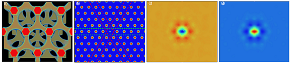
Figure 1 (a) Top view of the 3D photonic crystal with fcc lattice. It consists of alternating layers of a triangular lattice of air holes and a triangular lattice of silicon rods. (b) Horizontal cross section of the crystal. Dashed lines show the obvious paths atoms can travel. A defect is introduced by reducing the radius of the middle rod down to hold a single mode in the cavity. The (c) real part and (d) imaginary part of the electric field of the TM mode (wavelength 5.9mm, tuned to the atomic transition) allowed in the cavity at a particular instant in time.
Fig. 1 shows our design for a 3D PBG cavity which can be used as either an atomic entanglement source or quantum logic gates such as Hadamard, NOT, and SWAP. The single-mode of the cavity acts as a mediator for a coherent interaction between the two Rb atoms propagating through the void regions (dashed lines) of the photonic crystal structure. If the atoms and cavity satisfy certain physical conditions they manifest quantum logic operations.
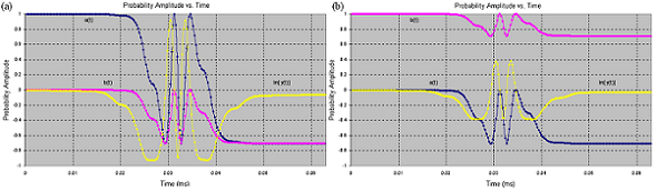
Figure 2 Probability amplitudes for entangled atoms produced by a dual-rail Hadamard operation in the 3D photonic crystal when (a) atom A is initially in the excited state and (b) atom B is initially in the excited state. Speed of the atoms is 353m/s.
In Fig. 2 we show how the atom-cavity interaction gives entanglement and the Hadamard logic operation. a(t), b(t), and gamma(t) are the probability amplitudes for the states |100> (atom A in the excited state) , |010> (atom B in the excited state) and |001> (cavity in the excited state), respectively. Probability amplitudes reach virtually asymptotic values shortly after the interaction and the cavity is disentangled from the atoms which leaves behind entangled states of the two atoms A and B. Similarly Fig. 3 shows the dual-rail NOT operation which can also be used as a single qubit SWAP gate.
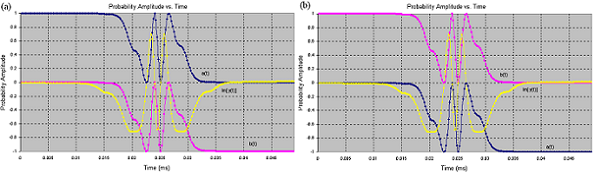
Figure 3 Probability amplitudes for atoms A and B under the dual-rail NOT operation in the 3D photonic crystal when initially (a) only atom A is excited and (b) only atom B is excited. Speed of the atoms is 459m/s.
Quantum Teleportation
We have also designed an integrated conditional quantum teleportation circuit and a readout circuit using a two-dimensional photonic crystal single chip which can be fabricated and tested with current or near future semiconductor process technology and experimental techniques. An illustration is shown in Fig. 4. Atom B, initially prepared in the excited state, is first entangled with an initially empty cavity by going through the horizontal trajectory in the teleportation circuit (TC). Then atom A, whose state is to be teleported, interacts with the cavity (diagonal trajectory). Subsequent detection of atom A in the excited state collapses atom B to the initial state of atom A. Next the readout circuit (RC) verifies if the atom is teleported correctly by employing the atom-waveguide interaction and a subsequent detection by another field-ionization detector.
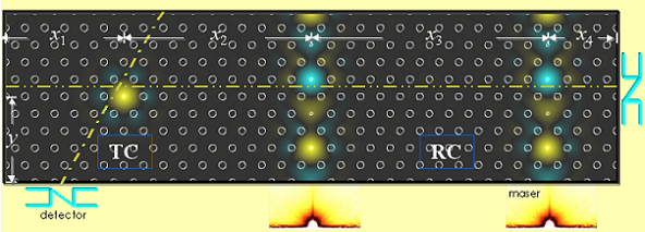
Figure 4 Illustration of the proposed photonic crystal quantum circuit. This illustration is not to scale. Actual dimensions are 17.4cm X 1.5cm.
The readout part of our device can also be used on its own or integrated with other compatible optical circuits to achieve atomic state detection. Further improvement of the device in terms of compactness and robustness could be achieved by integrating it with sources and detectors in the optical regime.
Metamaterials
Metamaterial structures, man-made and usually periodic with subwavelength feature sizes, enable a wide variety of exotic applications including invisibility cloaks [10], compact antennas [11,12] for mobile stations, quantum levitation [13], optical analogue simulators [14,15], solar photovoltaics [16], metaspacers [17], and many others. Furthermore, the interplay between metamaterials and surface plasmons in the optical region can lead to applications superior to conventional ones, such as ultra-high resolution imaging [18] and high-precision optical lithography [19].
Under sufficiently large wavelengths, many metamaterials can be approximated by a highly dispersive and lossy homogeneous medium with effective constitutive parameters [20–28]. Spontaneous and stimulated emission processes were studied using the quantization of the electromagnetic field in such dispersive dielectric materials [29] and negative index media [30,31], although the results were not generalized to inherently discrete metamaterial structures. When the wavelength of the external electromagnetic field is substantially smaller, the metamaterial structure cannot be approximated by an effective homogeneous medium anymore; rather it starts to behave as a photonic crystal [32]. The history of studying quantum processes in photonic crystals, which can be designed by low-loss materials unlike most metamaterials, is more extensive and richer compared to metamaterials [33,5,6].
On the other hand, in plasmonics, the effect of subwavelength hole arrays on the properties of polarization-entangled photons has been investigated [34]. Here, it was found experimentally that the two-particle entanglement survives transmission through such a medium, where the plasmonic arrays convert incident entangled photons first into localised surface plasmons and then back to free-space photons. The process was later described by classical scattering [35] and linear transformation theory [36]. The scattering theory approach was further used in Ref. [35] to determine the conditions on polarization-dependent transmission probabilities of photons in partially entangled Bell pairs for entanglement distillation. The quantum description of surface plasmons is now well established [37], and a quantum description of the photon-to-surface plasmon conversion process based on attenuated reflection [38,39] and the scattering of surface plasmon polaritons from a plasmonic beam splitter [40] have been developed, amongst many other schemes [37]. Most relevant to this work is the recent experimental demonstration of effective transduction of multimode quantum correlations achieved by employing localized surface plasmons in plasmonic subwavelength hole arrays [41].
As part of this project, we continue along the direction of subwavelength arrays and extend the entanglement distillation process in Ref. [35] to partially entangled multipartite systems [42], in particular, partially entangled 3-photon W states using plasmonic metamaterials [26,43]. We use the global entanglement measure defined in Ref. [44] to quantify the entanglement of the quantum states. This entanglement measure is scalable and can be applied to any number of two-level quantum particles.
Maximally entangled states are central resource for quantum information processing. However, due to decoherence and dissipation during their preparation, storage and distribution, entanglement between particles are degraded resulting in non-maximally entangled or partially mixed states. Entanglement protection, distillation, concentration or purification protocols are needed to extract highly entangled states from non-maximally entangled states. These protocols have been well-studied and experimentally demonstrated for bipartite entangled states [45–48]. As the number of particles forming entangled states increases, the entanglement structure becomes more complex and diverse, and inequivalent entanglement classes emerge. Among these W and GHZ states are the commonly studied multipartite entangled states. Recently, there has been several theoretical and experimental works on the efficient preparation, expansion and fusion of W states to build entanglement webs with large number of nodes [49–54]. Naturally, entanglement protection, distillation, purification and concentration protocols should be extended to such multipartite entangled states. Entanglement distillation schemes for partially entangled [55–57] and arbitrary [58–60] W states based on multiphoton [55–57,60] and single-photon multimode [58] entanglement concentration protocols have been theoretically proposed using linear [55,56,60] and nonlinear [57,58] optical elements, and coupled quantum dot and cavity systems [59]. While these protocols provide relatively more efficient distillation of less-entangled states, our approach provides a simple, fast and straightforward distillation of partially entangled Bell and 3-photon W states (see Fig. 5) without requiring any sophisticated protocols and their optical implementation.
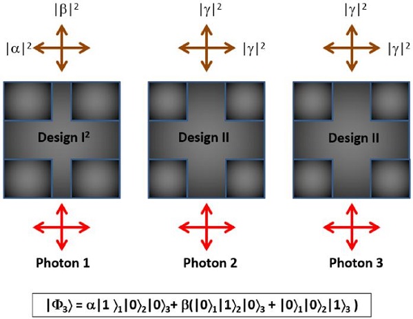
Figure 5 Distillation of partially entangled 3-photon W state described in the bottom. Each photon in the initial quantum state passes through different metamaterials. Two of the metamaterials have identical polarization independent designs. The required transmittance of all the metamaterials for each polarization state is shown in the top.
Acknowledgment
We collaborate with David A. Meyer (University of California, San Diego), Sahin Kaya Ozdemir (Washington University, St. Louis), Lan Yang (Washington University, St. Louis), Mark Tame (University of KwaZulu-Natal, South Africa), Martin Wegener (Karlsruhe Institute of Technology, Germany), Nobuyuki Imoto (Osaka University, Japan), and Takashi Yamamoto (Japan).
This project is currently funded in part by the National Science Foundation (NSF) under grant ECCS-1202443 and National Research Foundation, South Africa. In the past, this project was supported in part by the National Security Agency (NSA) and Advanced Research and Development Activity (ARDA) under Army Research Office (ARO) grant, by the Defense Advanced Research Project Agency (DARPA) Quantum Information Science and Technology (QuIST) program, and by the National Science Foundation (NSF).
References
[1] D. Awschalom, R. Clark, D. DiVincenzo, P. Chris Hammel, D. Steel, and K. B. Whaley, Solid-state approaches to quantum information processing and quantum computing, in A Quantum Information Science and Technology Roadmap, 2004, http://qist.lanl.gov.
[2] P. G. Kwiat, An integrated light circuit, Nature 453, 294 (2008).
[3] A. Politi, M. J. Cryan, J. G. Rarity, S. Yu, and J. L. O’Brien, Silica-on-silicon waveguide quantum circuits, Science 320, 646 (2008).
[4] P. Kwiat and G. Milburn, Optical approaches to quantum information processing and quantum computing, in A Quantum Information Science and Technology Roadmap, 2004, http://qist.lanl.gov.
[5] D. Ö. Güney and David A. Meyer, Creation of entanglement and implementation of quantum logic gate operations using a three-dimensional photonic crystal single-mode cavity, J. Opt. Soc. Am. B 24, 283 (2007).
[6] D. Ö. Güney and David A. Meyer, Integrated conditional teleportation and readout circuit based on a photonic crystal single chip, J. Opt. Soc. Am. B 24, 391 (2007).
[7] N. Vats and T. Rudolph, Quantum information processing in localized modes of light within a photonic bandgap material, J. Mod. Opt. 48, 1495 (2001).
[8] M. Konopka and V. Buzek, Entangling atoms in photonic crystals, Eur. Phys. J. D 10, 285 (2000).
[9] D. G. Angelakis and P. L. Knight, Testing Bell inequalities in photonic crystals, Eur. Phys. J. D 18, 247 (2002).
[10] D. Schurig, J. J. Mock, B. J. Justice, S. A. Cummer, J. B. Pendry, A. F. Starr, and D. R. Smith, “Metamaterial
electromagnetic cloak at microwave frequencies,” Science 314(5801), 977–980 (2006).
[11]. I. Bulu, H. Caglayan, K. Aydin, and E. Ozbay, “Compact size highly directive antennas based on the SRR
metamaterial medium,” New J. Phys. 7, 223 (2005).
[12]. H. Odabasi, F. Teixeira, and D. O. Güney, “Electrically small, complementary electric-field-coupled resonator
antennas,” J. Appl. Phys. 113(8), 084903 (2013).
[13]. U. Leonhardt and T. G. Philbin, “Quantum levitation by left-handed metamaterials,” New J. Phys. 9(8), 254
(2007).
[14] D. O. Güney and D. A. Meyer, “Negative refraction gives rise to the Klein paradox,” Phys. Rev. A 79(6),
063834 (2009).
[15] D. A. Genov, S. Zhang, and X. Zhang, “Mimicking celestial mechanics in metamaterials,” Nat. Phys. 5(9), 687–
692 (2009).
[16] A. Vora, J. Gwamuri, N. Pala, A. Kulkarni, J. M. Pearce, and D. O. Güney, “Exchanging Ohmic losses in
metamaterial absorbers with useful optical absorption for photovoltaics,” Sci Rep 4, 4901 (2014).
[17] M. I. Aslam and D. O. Güney, “On negative index metamaterial spacers and their unusual optical properties,”
Prog. Electromagn. Res. B 47, 203–217 (2013).
[18] J. B. Pendry, “Negative refraction makes a perfect lens,” Phys. Rev. Lett. 85(18), 3966–3969 (2000).
[19] T. Xu, Y. Zhao, J. Ma, C. Wang, J. Cui, C. Du, and X. Luo, “Sub-diffraction-limited interference
photolithography with metamaterials,” Opt. Express 16(18), 13579–13584 (2008).
[20] D. R. Smith, S. Schultz, P. Markos, and C. M. Soukoulis, “Determination of effective permittivity and
permeability of metamaterials from reflection and transmission coefficients,” Phys. Rev. B 65(19), 195104
(2002).
[21] X. Chen, T. M. Grzegorczyk, B.-I. Wu, J. Pacheco, Jr., and J. A. Kong, “Robust method to retrieve the
constitutive effective parameters of metamaterials,” Phys. Rev. E Stat. Nonlin. Soft Matter Phys. 70(1 Pt 2),
016608 (2004).
[22] D. R. Smith, D. C. Vier, T. Koschny, and C. M. Soukoulis, “Electromagnetic parameter retrieval from
inhomogeneous metamaterials,” Phys. Rev. E Stat. Nonlin. Soft Matter Phys. 71(3), 036617 (2005).
[23] J. Zhou, T. Koschny, M. Kafesaki, and C. M. Soukoulis, “Negative refractive index response of weakly and
strongly coupled optical metamaterials,” Phys. Rev. B 80(3), 035109 (2009).
[24] D. O. Güney, T. Koschny, M. Kafesaki, and C. M. Soukoulis, “Connected bulk negative index photonic
metamaterials,” Opt. Lett. 34(4), 506–508 (2009).
[25] D. O. Güney, T. Koschny, and C. M. Soukoulis, “Intra-connected three-dimensionally isotropic bulk negative
index photonic metamaterial,” Opt. Express 18(12), 12348–12353 (2010).
[26] M. I. Aslam and D. O. Güney, “Surface plasmon driven scalable low-loss negative-index metamaterial in the
visible spectrum,” Phys. Rev. B 84(19), 195465 (2011).
[27] M. I. Aslam and D. O. Güney, “Dual band double-negative polarization independent metamaterial for the visible
spectrum,” J. Opt. Soc. Am. B 29(10), 2839–2847 (2012).
[28] S. Arslanagic, T. V. Hansen, N. A. Mortensen, A. H. Gregersen, O. Sigmund, R. W. Ziolkowski, and O.
Breinbjerg, “A review of the scattering-parameter extraction method with clarification of ambiguity issues in
relation to metamaterial homogenization,” IEEE Antenn. Propag. M. 55(2), 91–106 (2013).
[29] P. W. Miloni, “Field quantization and radiative processes in dispersive dielectric media,” J. Mod. Opt. 42(10),
1991–2004 (1995).
[30] P. W. Milonni and G. J. Maclay, “Quantized-field description of light in negative-index media,” Opt. Commun.
228(1-3), 161–165 (2003).
[31] M. Ligare, “Propagation of quantized fields through negative-index media,” J. Mod. Opt. 58(17), 1551–1559
(2011).
[32] F. Dominec, C. Kadlec, H. Němec, P. Kužel, and F. Kadlec, “Transition between metamaterial and photoniccrystal
behavior in arrays of dielectric rods,” Opt. Express 22(25), 30492–30503 (2014).
[33] J. Vucković, M. Loncar, H. Mabuchi, and A. Scherer, “Design of photonic crystal microcavities for cavity
QED,” Phys. Rev. E Stat. Nonlin. Soft Matter Phys. 65(1 Pt 2), 016608 (2002).
[34] E. Altewischer, M. P. van Exter, and J. P. Woerdman, “Plasmon-assisted transmission of entangled photons,”
Nature 418(6895), 304–306 (2002).
[35] J. L. van Velsen, J. Tworzydlo, and C. W. J. Beenakker, “Scattering theory of plasmon-assisted entanglement
transfer and distillation,” Phys. Rev. A 68(4), 043807 (2003).
[36] E. Moreno, F. J. García-Vidal, D. Erni, J. I. Cirac, and L. Martín-Moreno, “Theory of plasmon-assisted
transmission of entangled photons,” Phys. Rev. Lett. 92(23), 236801 (2004).
[37] M. S. Tame, K. R. McEnery, S. K. Ozdemir, J. Lee, S. A. Maier, and M. S. Kim, “Quantum plasmonics,” Nat.
Phys. 9(6), 329–340 (2013).
[38] M. S. Tame, C. Lee, J. Lee, D. Ballester, M. Paternostro, A. V. Zayats, and M. S. Kim, “Single-photon excitation
of surface plasmon polaritons,” Phys. Rev. Lett. 101(19), 190504 (2008).
[39] D. Ballester, M. S. Tame, C. Lee, J. Lee, and M. S. Kim, “Long-range surface plasmon-polariton excitation at
the quantum level,” Phys. Rev. A 79(5), 053845 (2009).
[40] D. Ballester, M. S. Tame, and M. S. Kim, “Quantum theory of surface-plasmon polariton scattering,” Phys. Rev.
A 82(1), 012325 (2010).
[41] B. J. Lawrie, P. G. Evans, and R. C. Pooser, “Extraordinary optical transmission of multimode quantum
correlations via localized surface plasmons,” Phys. Rev. Lett. 110(15), 156802 (2013).
[42] M. A. al Farooqui, J. Breeland, M. I. Aslam, M. Sadatgol, S. K. Ozdemir, M. Tame, L. Yang, and D. O. Guney, Quantum entanglement distillation with metamaterials, Opt. Express 23, 17941 (2015).
[43] D. O. Güney, Th. Koschny, and C. M. Soukoulis, “Surface plasmon driven electric and magnetic resonators for
metamaterials,” Phys. Rev. B 83(4), 045107 (2011).
[44] D. A. Meyer and N. R. Wallach, “Global entanglement in multipartite systems,” J. Math. Phys. 43(9), 4273–
4278 (2002).
[45] T. Yamamoto, M. Koashi, S. K. Özdemir, and N. Imoto, “Experimental extraction of an entangled photon pair
from two identically decohered pairs,” Nature 421(6921), 343–346 (2003).
[46] P. G. Kwiat, S. Barraza-Lopez, A. Stefanov, and N. Gisin, “Experimental entanglement distillation and ‘hidden’
non-locality,” Nature 409(6823), 1014–1017 (2001).
[47] R. Reichle, D. Leibfried, E. Knill, J. Britton, R. B. Blakestad, J. D. Jost, C. Langer, R. Ozeri, S. Seidelin, and D.
J. Wineland, “Experimental purification of two-atom entanglement,” Nature 443(7113), 838–841 (2006).
[48] T. Yamamoto, K. Hayashi, S. K. Özdemir, M. Koashi, and N. Imoto, “Robust photonic entanglement
distribution by state-independent encoding onto decoherence-free subspace,” Nat. Photonics 2(8), 488–491
(2008).
[49] T. Tashima, S. K. Özdemir, T. Yamamoto, M. Koashi, and N. Imoto, “Local expansion of photonic W state
using a polarization-dependent beamsplitter,” New J. Phys. 11(2), 023024 (2009).
[50] T. Tashima, T. Wakatsuki, S. K. Özdemir, T. Yamamoto, M. Koashi, and N. Imoto, “Local transformation of
two Einstein-Podolsky-Rosen photon pairs into a three-photon w state,” Phys. Rev. Lett. 102(13), 130502
(2009).
[51] P. Walther, K. J. Resch, and A. Zeilinger, “Local conversion of Greenberger-Horne-Zeilinger states to
approximate W states,” Phys. Rev. Lett. 94(24), 240501 (2005).
[52] Ş. K. Özdemir, E. Matsunaga, T. Tashima, T. Yamamoto, M. Koashi, and N. Imoto, “An optical fusion gate for
W-states,” New J. Phys. 13(10), 103003 (2011).
[53] F. Ozaydin, S. Bugu, C. Yesilyurt, A. A. Altintas, M. Tame, and Ş. K. Özdemir, “Fusing multiple W states
simultaneously with a Fredkin gate,” Phys. Rev. A 89(4), 042311 (2014).
[54] T. Tashima, T. Kitano, Ş. K. Özdemir, T. Yamamoto, M. Koashi, and N. Imoto, “Demonstration of local
expansion toward large-scale entangled webs,” Phys. Rev. Lett. 105(21), 210503 (2010).
[55] B. Gu, D. Quan, and S. Xiao, “Multi-photon entanglement concentration protocol for partially entangled W
states with projection measurement,” Int. J. Theor. Phys. 51(9), 2966–2973 (2012).
[56] B. Gu, “Single-photon-assisted entanglement concentration of partially entangled multiphoton W states with
linear optics,” J. Opt. Soc. Am. B 29, 1685–1689 (2012).
[57] F.-F. Du, T. Li, B.-C. Ren, H.-R. Wei, and F.-G. Deng, “Single-photon-assisted entanglement concentration of a
multiphoton system in a partially entangled W state with weak cross-Kerr nonlinearity,” J. Opt. Soc. Am. B
29(6), 1399–1405 (2012).
[58] L. Zhou, Y.-B. Sheng, W.-W. Cheng, L.-Y. Gong, and S.-M. Zhao, “Efficient entanglement concentration for
arbitrary single-photon multimode W state,” J. Opt. Soc. Am. B 30(1), 71–78 (2013).
[59] Y. B. Sheng and L. Zhou, “Efficient W-state entanglement concentration using quantum-dot and optical
microcavities,” J. Opt. Soc. Am. B 30(3), 678–686 (2013).
[60] T. J. Wang and G. L. Long, “Entanglement concentration for arbitrary unknown less-entangled three-photon W
states with linear optics,” J. Opt. Soc. Am. B 30(4), 1069–1076 (2013).