Edward M. Nadgorny - Research Projects
Dislocation Engineering in Si

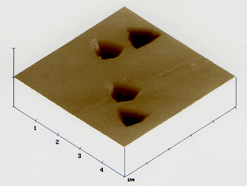
The picture below shows an array of four dislocations
selectively etched on a {111} Si substrate (AFM image, Nanoscope Dimension 3000 SPM, Digital
Instruments). The dislocations were introduced into a dislocation-free 0.4-mm substrate by local
deformation and bending at about 900 K; they were revealed by selective dislocation etching.
Nadgorny's Home Page |
Physics Home