
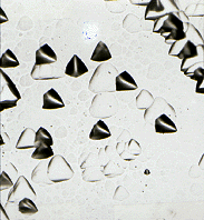
 ....The selective etching of dislocations in silicon allows one to see dislocation structure of Si
single crystals after any modification or treatment, such as cutting, grinding, polishing, thermal
treatment or deformation. The differently oriented triangles in the picture of a
selectively etched {111} silicon surface correspond to dislocations moved
in different glide systems.
....The selective etching of dislocations in silicon allows one to see dislocation structure of Si
single crystals after any modification or treatment, such as cutting, grinding, polishing, thermal
treatment or deformation. The differently oriented triangles in the picture of a
selectively etched {111} silicon surface correspond to dislocations moved
in different glide systems.
Nadgorny's Home Page |
Physics Home